A 555 timer is a small, versatile integrated circuit that can turn a few basic components into a flashing LED, pulse generator, or simple delay. Building a 555 Ic Timer Circuit is a practical way to learn how resistors and capacitors shape an electronic signal. The parts are familiar: a 555 chip, a breadboard, jumper wires, an LED, a current-limiting resistor, and a timing capacitor. Start with a blink.
This introduction focuses on the common astable configuration, where the timer repeatedly switches its output on and off. You will learn what each important pin does, how to connect the timing components, and how to estimate the flash rate. The familiar timing formula is a useful starting point, not a promise of perfect accuracy. Component tolerances, wiring, and the specific 555 variant can all affect the result.
Small details matter. Check the pin-one mark before placing the chip, observe the LED’s polarity, and confirm the supply voltage against the datasheet for your exact device. Disconnect power before changing breadboard connections. Then test the circuit and compare its actual timing with your estimate. It may blink too quickly. That is useful evidence, not failure: measure the result, review the component values, and adjust one part at a time. A first build can feel untidy, and the explanation may not answer every question. Careful observation makes the next revision clearer and more reliable.
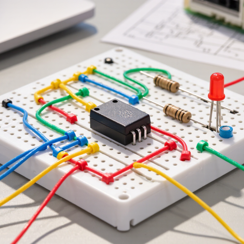
A 555 timer is an eight-pin integrated circuit that changes its output when capacitor voltage crosses internal thresholds. Inside, comparators control a latch, while a discharge transistor helps charge or empty the timing capacitor. That simple arrangement supports several useful operating modes. A pinout diagram helps prevent wiring mistakes.
Monostable mode produces one timed pulse after a trigger. A resistor and capacitor set its approximate duration; component tolerances can shift the result.
Astable mode repeatedly switches between high and low, creating a square wave. Two resistors and one capacitor set its timing, though the high and low periods may differ.
Bistable mode acts like a basic set-reset latch. A brief input can change its output, which stays put until another input arrives.
When assembling a circuit, check the pin connections and supply-voltage limits in the specific device’s datasheet. Place a small bypass capacitor near the supply pins to reduce unwanted switching noise. Keep timing leads short, especially around the capacitor.
Small detail.
A common bench mistake is choosing a capacitor without considering leakage or tolerance. I still find it useful to measure the actual timing, rather than trusting a calculation alone. A simple LED can show the output changing, but its resistor must limit current.

For a basic 555 timer circuit, choose the operating mode before buying parts. An astable setup repeatedly switches its output on and off, making it useful for a blinking LED or simple tone. It needs two resistors and one timing capacitor. Connect RA between the supply and pin 7, RB between pin 7 and pins 2 and 6, and the capacitor from pins 2 and 6 to ground. A 10 kΩ RA, 47 kΩ RB, and 10 µF capacitor produce roughly 1.4 pulses per second. The estimate uses f ≈ 1.44 ÷ ((RA + 2RB) × C). Keep resistor values within sensible limits, and check the timer’s datasheet for operating voltage and pin ratings.
Component tolerances affect the actual timing. A capacitor marked 10 µF may not measure exactly 10 µF, especially if it is electrolytic; observe its polarity. For steadier operation, place a 100 nF bypass capacitor close to the timer’s supply and ground pins. A small capacitor from pin 5 to ground can reduce noise, though many simple builds work without it. Keep the wiring short. That helps. If an LED is connected to the output, include a current-limiting resistor. The first frequency calculation is only a starting point; measure the output and adjust RB or the capacitor if the timing feels off. My own instinct would be to change one component at a time, though it can be tempting to swap several at once.
When reading a 555 timer schematic, identify the package notch before tracing wires. Viewed from above, pin 1 sits beside the notch; numbering continues down one side and up the other. Pin 1 connects to ground, while pin 8 connects to the positive supply. Pin 3 is the output. Check the drawing’s pin numbers rather than relying on how the chip appears on the page.
For a common astable circuit, pins 2 and 6 join at the timing node. A capacitor runs from this node to ground. One resistor connects the supply to pin 7, and another connects pin 7 to the joined pins 2 and 6. Pin 4, the active-low reset, usually connects to the supply so the timer can run. Pin 5 is the control-voltage input; a small capacitor from pin 5 to ground can help reduce noise. Keep the wiring clear. Those shared nodes are easy to misread.
Before applying power, compare every connection with the schematic. Place a small bypass capacitor between pins 8 and 1, close to the chip. I sometimes redraw crowded junctions by hand; it feels slower, but it catches mistakes. Confirm the supply voltage against the specific timer’s datasheet, and avoid drawing more output current than the device can safely provide.
Place the 555 timer across the breadboard’s center gap, with its notch facing one end. This keeps each pair of chip pins in separate rows. Connect pin 1 to the ground rail, and pin 8 to a regulated 5–9 V supply. Join pin 4 to the positive rail so reset stays inactive. Check whether the power rails are split halfway; some boards need extra jumper wires.
For a simple blinking circuit, connect a resistor from positive to pin 7, then another resistor from pin 7 to pins 2 and 6, joined together. Add a timing capacitor between pins 2 and 6 and ground, observing its polarity if it is electrolytic. A small ceramic capacitor from pin 5 to ground can help steady the circuit. Add a 100 nF decoupling capacitor close to pins 8 and 1. Connect pin 3 to an LED through a current-limiting resistor, with the LED’s other lead going to ground.
Small details matter.
Check every connection before applying power. A jumper may look seated but miss its contact. If the LED stays dark, inspect the chip’s orientation, capacitor polarity, and shared breadboard rows before changing components. A slow blink is normal with larger timing values. I’d still verify the supply voltage with a meter, since a weak connection can make the circuit behave oddly.
With power disconnected, inspect the 555 timer’s orientation, breadboard rails, and capacitor polarity. Then apply a stable 5 V supply and measure the output at pin 3 with an oscilloscope or multimeter. In astable mode, the output should switch between low and high levels. The trigger and threshold inputs respond near one-third and two-thirds of the supply voltage. Check the timing capacitor voltage too; it should rise and fall rather than remain flat. Check the rails.
If the output stays fixed, look for a misplaced timing resistor, a short between adjacent rows, or a reset pin held low. Compare the measured period with the estimate: T ≈ 0.693 × (RA + 2RB) × C. Component variation can explain a mismatch. IEC 60063 defines the E24 preferred-value series for 5% resistors, while capacitor tolerance can be wider. NIST Technical Note 1297 explains how measurement uncertainty affects reported results. Record the supply voltage and component values before changing parts; otherwise, troubleshooting becomes guesswork. I would still question a reading taken with loose probes.
Tips: Use short ground leads, test one change at a time, and confirm the capacitor’s printed value. If timing drifts, swap in a known-good capacitor before rebuilding the circuit.
| Test or Symptom | Expected Observation | Possible Cause | Check or Corrective Action |
|---|---|---|---|
| Verify the supply voltage | Measure the intended supply voltage between pin 8 (VCC) and pin 1 (GND). A standard bipolar NE555 is commonly operated from about 4.5 V to 16 V; check the specific device datasheet. | No supply, reversed polarity, a weak battery, or a short circuit. | Confirm pin 8 is connected to positive supply and pin 1 to ground. Check the supply at the IC while the circuit is running. |
| Check the reset pin | Pin 4 (RESET) should normally be held high, close to VCC, for continuous operation. | Pin 4 is floating or held low, keeping the timer reset. | Connect pin 4 to VCC if reset control is not being used. If it is controlled externally, verify that the control signal goes high during operation. |
| Measure the timing capacitor voltage | In astable mode, the voltage at the timing capacitor should repeatedly rise toward about two-thirds of VCC and fall toward about one-third of VCC. | Incorrect capacitor wiring, an open or shorted capacitor, or a wiring error at pins 2, 6, or 7. | Check that pins 2 and 6 connect to the timing-capacitor node and that the capacitor returns to ground. Confirm pin 7 connects to the resistor junction. |
| Output remains constantly high or low | Pin 3 (OUT) should switch between low and high states while the astable circuit is oscillating. | Reset is low, timing components are miswired, the capacitor cannot charge or discharge, or the output is overloaded. | Check pin 4, the pin 2/6/7 connections, and the capacitor polarity if it is electrolytic. Disconnect the output load temporarily and retest. |
| Oscillation is too fast or too slow | For the example values, the approximate frequency is 4.8 Hz, using f ≈ 1.44 / ((RA + 2RB) × C). Actual frequency varies with component tolerances. | Wrong resistor or capacitor values, poor component connections, or normal component tolerance. | Measure or verify RA, RB, and C. Recalculate the expected frequency with the values actually installed; use an oscilloscope or frequency meter for a more reliable reading. |
| Output frequency is correct, but the duty cycle is unexpected | With the basic two-resistor astable circuit, the output is usually high longer than it is low. For equal RA and RB, the ideal high-time fraction is about two-thirds. | The basic astable arrangement does not produce a 50% duty cycle; resistor values also affect the timing intervals. | Check the resistor values and wiring. If a duty cycle near 50% is required, use a suitable diode-modified timing network or another circuit arrangement designed for that duty cycle. |
| Output voltage looks weak or distorted | The output should switch clearly between low and high levels, but its exact voltage depends on the timer version, supply, and load. | Excessive output current, a shorted load, or a supply that drops under load. | Remove or reduce the load and measure pin 3 again. Do not assume the output can directly drive a load that exceeds the device’s rated output current. |

| Unstable timing or erratic triggering | The circuit should oscillate consistently, with repeatable timing-capacitor ramps and output transitions. | Loose connections, electrical noise, long wiring, or inadequate supply decoupling. | Use short connections and add a 100 nF bypass capacitor between pins 8 and 1 near the IC. A 10 nF capacitor from pin 5 (CONTROL) to ground can help reduce noise when recommended by the circuit design. |
| Confirm the output waveform | An oscilloscope should show a rectangular waveform at pin 3 and a ramping waveform at the timing-capacitor node, cycling between approximately one-third and two-thirds of VCC. | Incorrect probe grounding, a wiring fault, or a measurement setup that loads the circuit. | Connect the oscilloscope ground to circuit ground and probe pin 3 and the capacitor node separately. Use a high-impedance probe where available. |


We offer Packaging Boxes delivered to your door. Secure, professional, and affordable, our custom made packaging boxes are guaranteed to protect and transport your valuable items. Our devoted team is always there to serve you.